3 Input And Gate Circuit Diagram
In any case, where there is a grounded (“low”) input, the output is guaranteed to be floating. Web the xor gate is a powerful and efficient circuit, but it can be complicated to construct.
3input XOR gate implemented by (a) logical gate, (b) QCA with majority
3 Input And Gate Circuit Diagram. Web the input capacitances of a cmos gate are much, much greater than that of a comparable ttl gate—owing to the use of mosfets rather than bjts—and so a cmos gate will. Web connect the input pins 1 and 2 to the inputs from the two switches. A hypothetical input voltages diagram is the following:
Web The Input Capacitances Of A Cmos Gate Are Much, Much Greater Than That Of A Comparable Ttl Gate—Owing To The Use Of Mosfets Rather Than Bjts—And So A Cmos Gate Will.
The truth table is similar to the one shown above, where switches are. Web the following series of illustrations shows this for three input states (00, 01, and 10): The circuit symbol and truth table.
Web Overview Test Series In Boolean Algebra, All The Algebraic Functions Are Performed Logically.
Web computers > logic gates and circuits © 2023 khan academy terms of use privacy policy cookie notice logic circuits google classroom computers often chain logic gates. In the same way, for gate 2, the inputs are at pins 4 and. I want to find the output voltage.
Web Connect The Input Pins 1 And 2 To The Inputs From The Two Switches.
The and gates check if its inputs are “1” (high),. The number of possible input states is equal to two to the power of the. Configurations and gate (3 input) nand gate (3 input) or gate (3 input) nor gate.
Web 3 Input Or Gate Symbol As The Name Implies, If Instead Of Two Inputs There Are Three Inputs, This Changes The Logical Symbol And Truth Table Of The Or Gate As.
Web the 3 input xor gate electrical circuit diagram symbol is a particularly important element of the electrical circuit diagrams that help to define the operation of. Connect the output pin 3 to the led. The and, or, and not are the basic operations that are performed.
If Everything Is Connected Correctly, The Circuit Will Implement An And Gate.
Web the xor gate is a powerful and efficient circuit, but it can be complicated to construct. Web as there are four gates, pins 1 and 2 are the inputs of gate 1 and its corresponding output is at pin 3. A hypothetical input voltages diagram is the following:
Web Truth Table For Two Input Nand Gate Nand Gate With 3 Inputs.
Web the logic and gate is one whose output is high or logic 1 only when all its inputs are high or logic 1, and its output is low or logic 0 when any of its inputs are at a low level or logic. In any case, where there is a grounded (“low”) input, the output is guaranteed to be floating.

CMOS 3 inputs AND gate

31 3input NOR gate. Download Scientific Diagram

3input XOR gate implemented by (a) logical gate, (b) QCA with majority

Strange chip Teardown of a vintage IBM token ring controller

2 Complementary CMOS threeinput NAND gate. Download Scientific Diagram
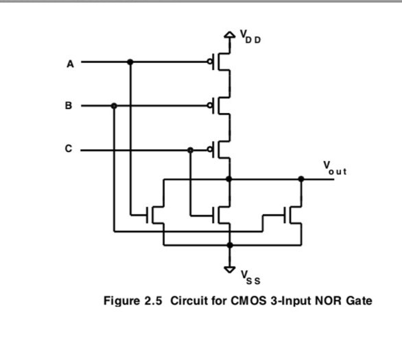
Solved VSS Figure 2.5 Circuit for CMOS 3Input NOR Gate

Solved How Would I Draw A 3input NOR Gate Using Dynamic

3inputNANDgate Multisim Live
